MATERIALS
Electricity in solids
- Good conductors, often just called Conductors, allow electrons to move freely.
- Poor conductors, often called Semiconductors, do not allow electrons to move freely.
- Non-conductors, often called Insulators, allow no movement of electrons.
The outer electrons are shielded from the nucleus by those closer to the nucleus.
It is these outer electrons that are responsible for the electrical properties of solids.
Conductors
All metals are good conductors of electricity.
The only non-metal that is a good conductor at room temperature is Graphite (Carbon).
Neutral atoms have the same number of electrons and protons, so that there is no net electric charge.
A metal atom has one or more outer electrons that are very weakly held in place by the nucleus.
In a solid, the metal atoms are fixed in place, but the outer electrons have sufficient thermal energy to move 'freely' around the solid.
These electrons are often referred to as Conduction electrons.
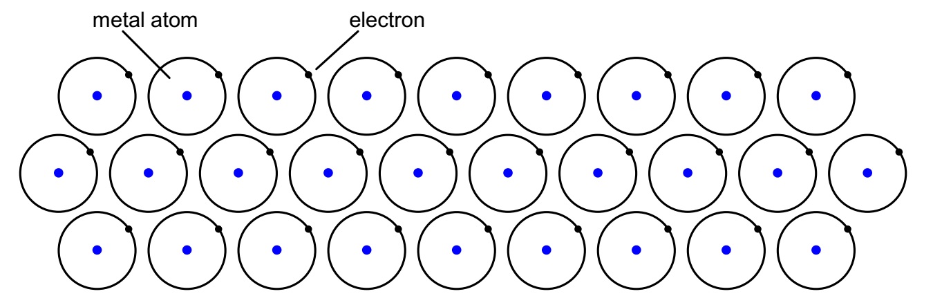
In a conductor, the number of conduction electrons is large.
Copper metal atoms have one outer electron that can move around.
One mole of copper atoms has a mass of 6.35 × 10⁻²kg.
The density of copper is 8.9 × 10³kgm-3.
Show that in one m3 there are ≈ 8.44 × 1028 conduction electrons.
The conduction electrons move very quickly.
Their speed can be estimated by equating their kinetic energy to their thermal energy.
=> ½mv2 = kT
where k is the Boltzmann constant,T is the absolute temperature,
m is the mass of an electron,
v is the velocity of an electron.
Show that the approximate velocity is 105ms-1.
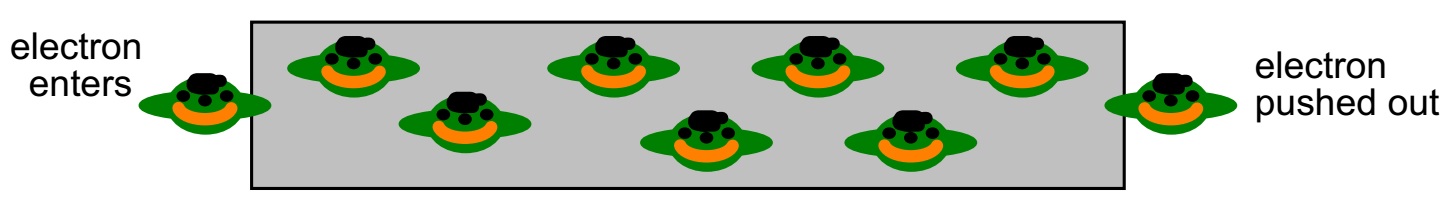
However, the speed that the conduction electrons drift along a conductor is low.
If a potential difference is put across the metal then the conduction electrons
will drift along the wire from the negative side and towards the positive side.
Consider a length, d, of wire of cross-sectional area, A,
made from a metal with n freely moving conduction electrons per cubic metre.
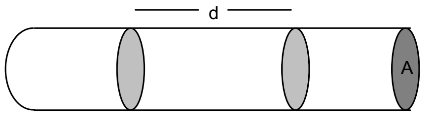
where v is the drift velocity, and e is the electronic charge.
Show that for copper, if I = 1 amp and A = 1mm2 then v ≈ 7.4 × 10⁻⁵ms-1
Why is there is there no significant delay when a light switch is operated?
Think of a hose pipe
Resistance
When a current flows in a metal, the electrons interact with both themselves and the fixed metal ions.
This impedes their progress and causes resistance.
(Consider moving through a crowd of people!)
This leads to a loss in energy which often results in an increase in temperature of the conductor.
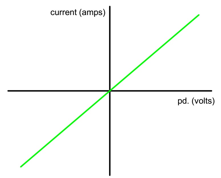
Georg Ohm found that the current through a wire was proportional to the PD across the wire,
so long as the temperature of the wire did not change.
So a graph of current v PD. is a straight line, i.e. the wire has a constant resistance.
(The PD is the independent variable and so on the 'x axis', - no PD, no current!)
If the temperature increases, then two things happen.
- outer electrons gain more thermal energy,
- metal atoms vibrate with a larger amplitude.
The metal atoms are now occupying a larger volume, they interact more with the conduction electrons.
This increases the resistance of the metal.
This can be seen by measuring the current passing through a filament lamp as the pd. is varied.
Filament lamp
The temperature of the metal filament will change from room temperature (e.g. 20°C) to over 1000°C when the lamp is switched on.
How could you measure the resistance of the hot filament?
The more opportunity that the electrons moving in a current have to interact with both themselves and the fixed metal ions, the greater the loss in energy and the larger the resistance.
Effect of length, (L)? Why? (series circuit)
Effect of thickness, (A)? Why? (parallel circuit)
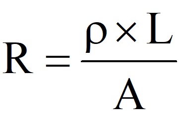
These two properties can be combined together to give R ∝ L/A
The constant of proportionality has the symbol ρ (rho) and is a property of the material.
How can we find the units of ρ?
Materials can be roughly classified according to their resistivity
- conductors 10-2 to 10-8Ωm
- semiconductors 10-6 to 106Ωm
- insulators 1011 to 1019Ωm
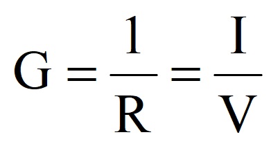
A term related to resistance is Conductance with the symbol G.
Conductance = 1 / resistance and has units of Siemens (S) or sometimes mohs.
The units of conductivity are Siemens/metre Sm-1.
Insulators and semiconductors
If a material has no free electrons, then no current is able to flow.
Any electrons that are put onto the material will remain where they are put - Static Electricity.
Pure Carbon, in the form of diamond, is an excellent insulator.
The diagram below is a 2D representation.
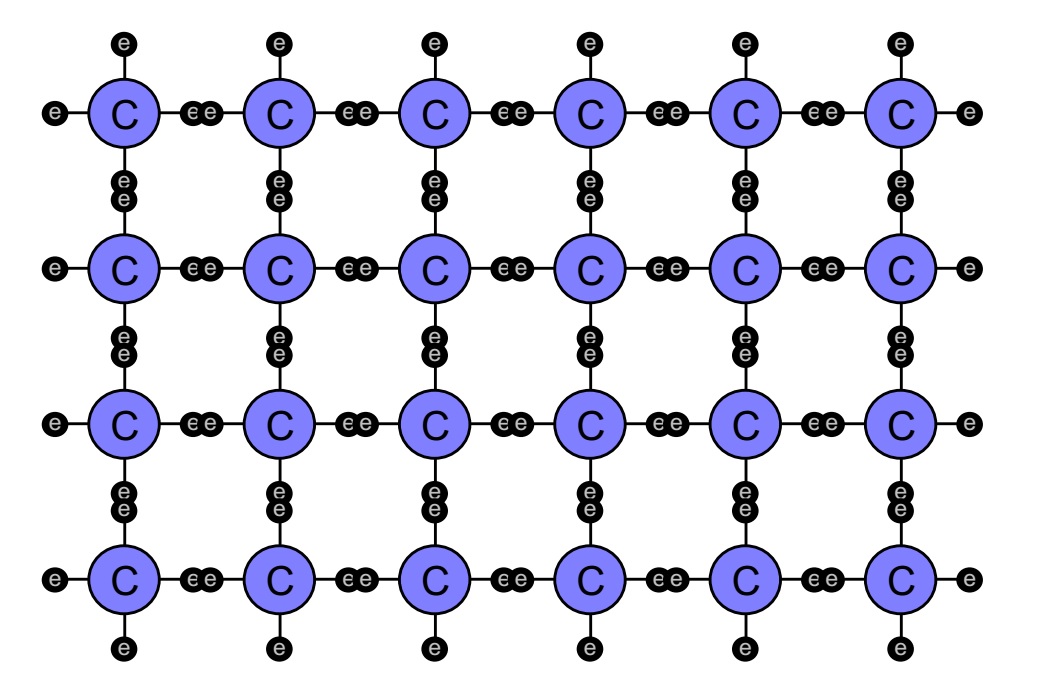
It requires a temperature of around 5000°C for these electrons have sufficient energy to become 'free'.
The resistivity of diamond at room temperature is around 1016Ωm.
Pure Silicon has a crystal structure similar to carbon but the electrons do not form such strong covalent bonds.
At a temperature of around 350°C, they become free.
So at room temperature, there are a few electrons with sufficient energy to break free and move around.
The diagram below is a 2D representation.
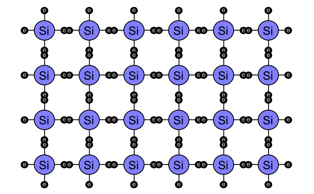
The resistivity of pure silicon at room temperature is around 104Ωm.
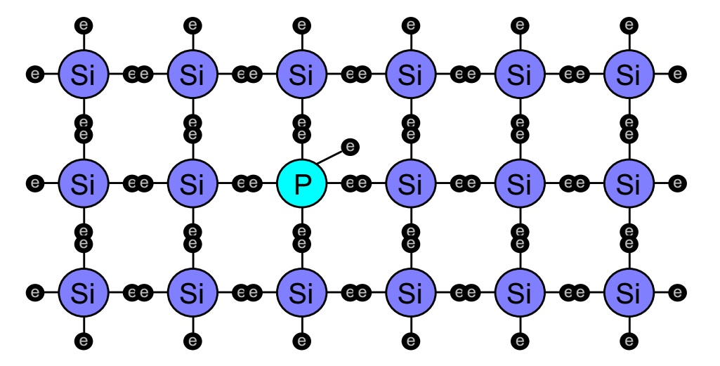
If there are impurities in the silicon, then the situation changes significantly.
The Field Effect Transistor (FET, on which modern digital computers are based) was patented in Britain in 1935 by Oskar Heil.
It could not be made because silicon could not be made with sufficient purity!
What if a phosphorus atom is added to a silicon crystal?
Phosphorus has 5 electrons in the outer part of the atom.
Silicon with phosphorus impurity
What will happen?
Silicon treated with impurities in this way is said to be 'doped'.
If the doping produces electrons that can move, the material is called an n-type semiconductor.
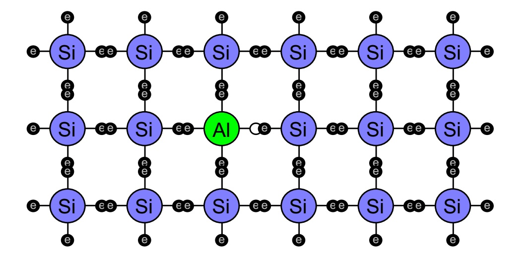
Consider adding an aluminium atom to a silicon crystal.
Aluminium has 3 electrons in the outer part of the atom.
Silicon with aluminium impurity
What will happen?
Silicon doped in this way is called an p-type semiconductor.
The amount of impurity added is very small and ranges from 1 part per 1012 to 1 part in 106.
The resistivity of doped silicon ranges from around 10Ωm to 10-6Ωm.
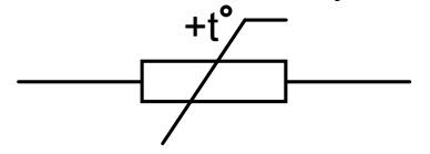
Doped silicon has several important uses including devices called Thermistors.
There are two main types:
- negative temperature coefficient, ntc
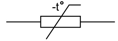 .
.- positive temperature coefficient, ptc
 .
.ntc
These are often made from lightly doped semiconductors.
As the temperature increases, more electrons become 'free' and so the resistance decreases.
The range of resistance can be altered at manufacture by changing the amount and type of doping agent.
A graph of resistance v temperature is non-linear. What will it look like?
ptc
These are often made from highly doped semiconductors.
As the temperature increases, the effect of the additional 'free' electrons is small compared to number of interactions of the electrons with the more vigorously vibrating ions, so making the resistance increase.
The range of resistance can be altered at manufacture by changing the amount and type of doping agent.
A graph of resistance v temperature is non-linear. What will it look like?
Light Dependent Resistors
LDR
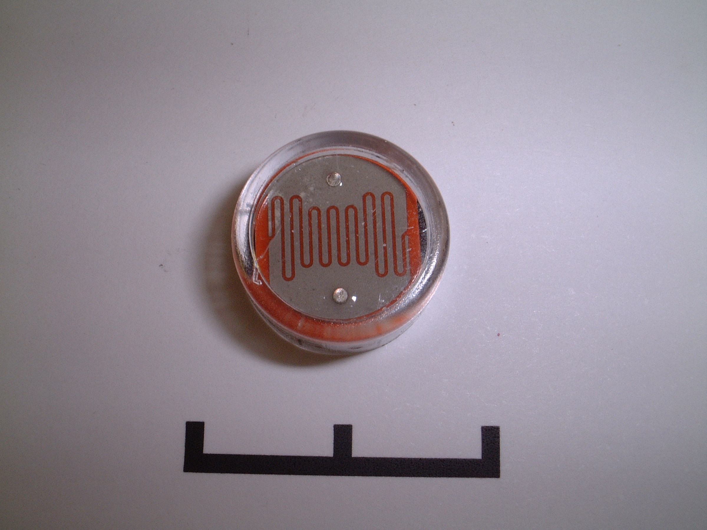
Some materials behave directly as semiconductors.
It was discovered in the 1920s that Cadmium Sulphide is such a material and has a 'band gap' of 2.42eV.
How does this compare to compare to the photon energy of visible light?
Cadmium sulphide is used to make LDRs.
How would you expect the resistance of an LDR to vary with light intensity?
The p-n junction
Semiconductors become particularly interesting when a p-type and n-type are formed together to produce a junction.
Before the junction is formed, the p-type and n-type semiconductors have no net charge. (Important!)
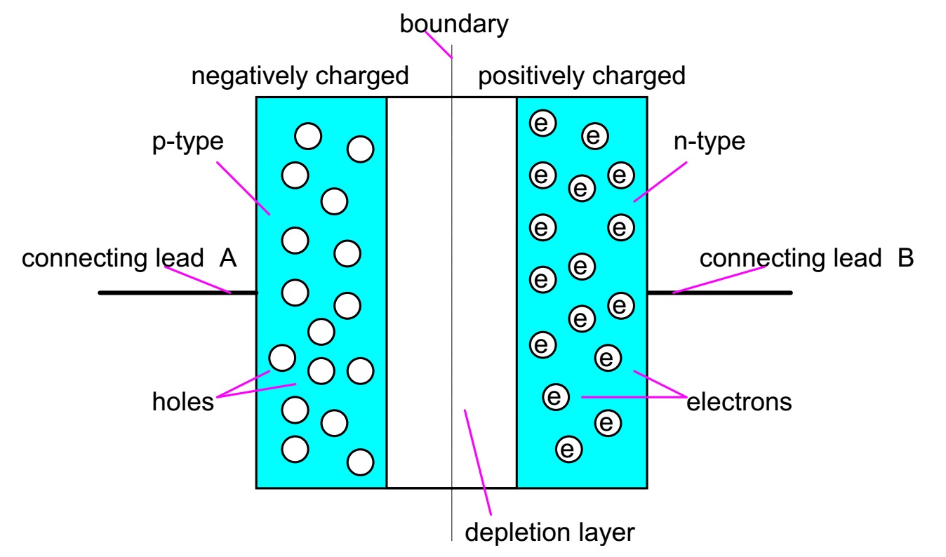
=> the p-type material becoming negatively charged (because it has gained electrons).
=> the n-type material becoming positively charged (because it has lost electrons).
=> the negative charge of the p-type repels any further electrons from moving across the boundary.
A region is left around the boundary where there are no holes or electrons, i.e. no free charge carriers.
This region is known as the Depletion Layer and is an insulator, i.e. no current can flow.
What if a PD is put across the p-n junction, with connecting lead A negative with respect to connecting lead B?
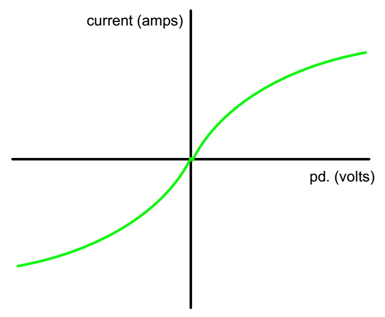
In this state, the p-n junction is said to be reversed biased.
What will happen if the PD continues to increase?
The maximum PD that can be put across a p-n junction depends on how it is made - a few volts up to many kilovolts.
What if a PD is put across the p-n junction, with connecting lead A positive with respect to connecting lead B?
If the pd. is increased, the depletion layer will eventually disappear, current can freely pass through the junction.
For silicon, the PD needed is around 0.7V.
In this state, the p-n junction is said to be forward biased.
A p-n junction used in this way forms a device called a Diode.
The symbol for a diode is
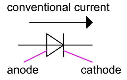
NOTE the different scale on the positive and negative PD axis
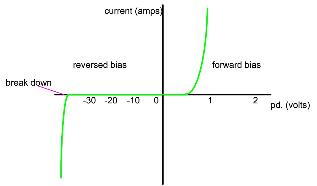
What happens in the p-n junction when reverse biased?
What happens in the p-n junction when forward biased?
Forward biased diode formula

I = the forward bias current,
I0 = the reverse bias current, (10-11A)
e = the charge on the electron,
V = the forward bias PD,
k = Boltzmann constant,
T = the absolute temperature.
Calculate I when V = 0.6V and T = 293K
Rearrange diode formula so that V is the subject.
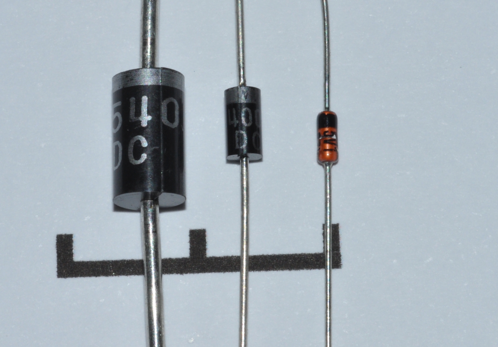
Types and uses
Some diodes, Bridge rectifiers
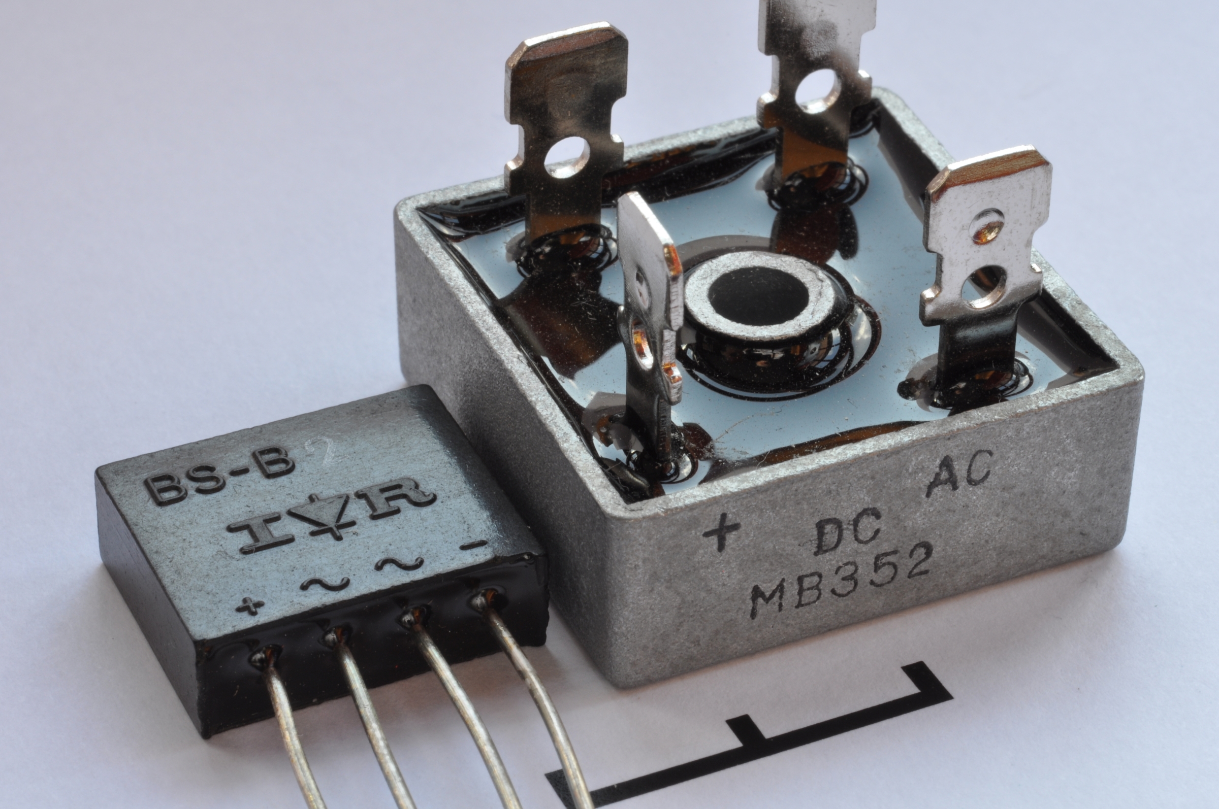
Diodes only allows current to flow in one direction => can control the direction that current passes in a circuit.
Mains electricity is alternating current (a.c.), but electronic circuits need direct current (d.c.) which only flow in one direction.
How are diodes used to change a.c. to d.c.?
Other types of diodes
Light Emitting Diodes (LEDs)
Photo Diodes
Zener diodes
Particle detectors